The 74×241 (ex 74LS241) is a cool little chip that has two 3-state buffers. One active low, one active high output enable.
In this guide, you will learn everything you need to know about this chip and how you can use unknowns in your own projects.
What does the 74HC241 / 74LS241 do?
The 74×241 gives you two inverting 3-state buffers. One with an active low Output Enable (OE), and one active high Output Enable (OE).
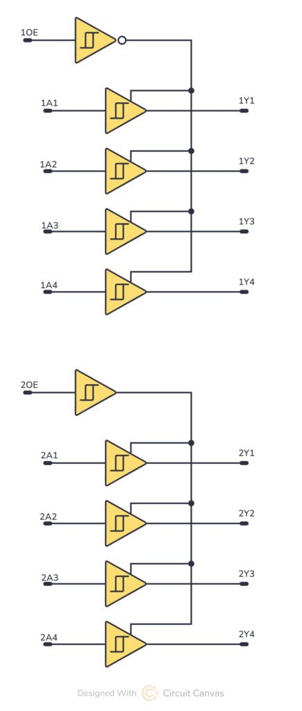
This is very similar to the 74LS244, just that the second Output Enable pin is active high on this chip.
How To Use This Chip
The 74HC241 comes in a 20-pin package, and you need to connect it to power before you can use it. Most 7400 ICs support a VCC voltage of 5V. One difference between the HC and LS version of the chip is that the 74HC241 supports 2V to 6V, while the 74LS241 only supports 5V.
74HC chips can normally supply a maximum of 6 mA from an output pin. If you’re using the 74LS version, the maximum current you can pull out of one output pin is 15 mA when the pin is high (sourcing) or 24 mA when the pin is low (sinking).
But these values can differ between models, so check the datasheet of your model to verify.
Once you’ve connected it to power, you can use the unknown inside.
10 Simple Steps to Learn Electronics
Electronics is easy when you know what to focus on and what to ignore. Learn what "the basics" really is and how to learn it fast.
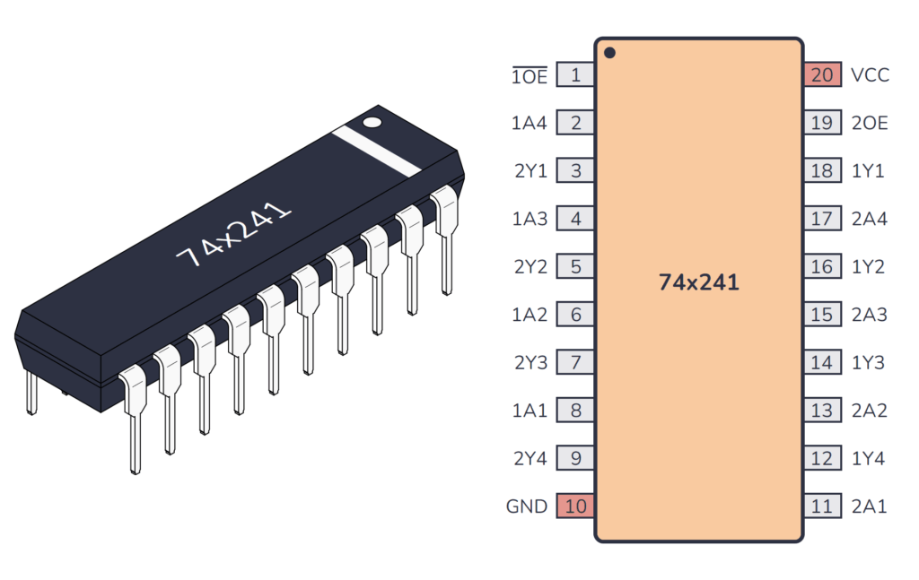
74×241 Pinout
The 74×241 has 20 pins and contains One active low, one active high output enable laid out as shown in the pinout diagram below:
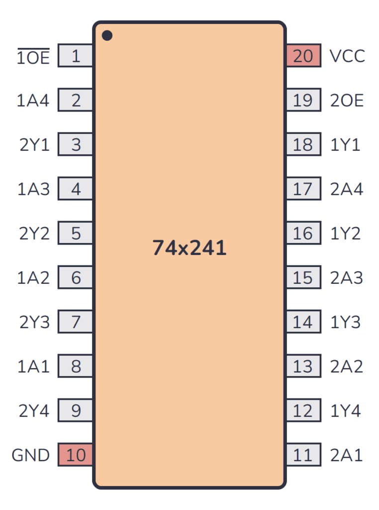
| Pin Name | Pin # | Type | Description |
|---|---|---|---|
| 1OE | 1 | Input | Output Enable for bus line 1 (active low). |
| 1A4 | 2 | Input | Data input for first buffer line 4. |
| 2Y1 | 3 | Output | Data output from second buffer line 1. |
| 1A3 | 4 | Input | Data input for first buffer line 3. |
| 2Y2 | 5 | Output | Data output from second buffer line 2. |
| 1A2 | 6 | Input | Data input for first buffer line 2. |
| 2Y3 | 7 | Output | Data output from second buffer line 3. |
| 1A1 | 8 | Input | Data input for first buffer line 1. |
| 2Y4 | 9 | Output | Data output from second buffer line 4. |
| GND | 10 | Power | Connect to ground (GND). |
| 2A1 | 11 | Input | Data input for second buffer line 1. |
| 1Y4 | 12 | Output | Data output from first buffer line 4. |
| 2A2 | 13 | Input | Data input for second buffer line 2. |
| 1Y3 | 14 | Output | Data output from first buffer line 3. |
| 2A3 | 15 | Input | Data input for second buffer line 3. |
| 1Y2 | 16 | Output | Data output from first buffer line 2. |
| 2A4 | 17 | Input | Data input for second buffer line 4. |
| 1Y1 | 18 | Output | Data output from first buffer line 1. |
| 2OE | 19 | Input | Output Enable for bus line 2 (active high). |
| VCC | 20 | Power | Positive power supply. Connect to +5V power. |
Alternatives and Equivalents for 74HC241 / 74LS241
There are many versions of the 74×241 chip. They all have the same functionality, but with different specifications such as supported voltages and maximum current output.
Here’s a list of a few equivalents of this chip:
- 74HC241 (High-speed CMOS)
- 74HCT241 (High-speed CMOS, TTL compatible)
- 74LS241 (High-speed TTL)
- 74LVC241 (Low Voltage TTL)
- 74AC241 (Advanced CMOS)
- 74ALS241 (Advanced Low-Power Schottky TTL)
- 74F241 (Very High Speed)
- 74C241 (CMOS, similar to the 4000-series)
Some manufacturers also add a prefix, such as the SN74HC241 and SN74LS241 by Texas Instruments.
Can’t find the 74×241 anywhere? Then try one of the following IC alternatives:
- 74×240 – Octal buffer/line driver with inverted outputs.
- 74×244 – Octal buffer/line driver with non-inverted outputs.
- 74×245 – Octal bus transceiver with non-inverted outputs.
- 74×541 – Octal buffer/line driver with 3-state outputs.
- 74×640 – Octal bus transceiver.
- 74×645 – Octal bus transceiver with inverted outputs.
- CD4503 – Hex non-inverting 3-state buffer.
If you can’t find the 74×241 IC in your local electronics store, don’t worry, you’ll most likely find it in one of the stores listed on this page of online stores where you’ll find components and tools for all your electronics projects.
Datasheet for the 74LS241 and 74HC241 chips
Download the PDF datasheet for your version of the 74×241 here:
Get the 555 Timer Cheatsheet
A super helpful reference that makes it easy to design circuits, so that you can build oscillators, timer circuits, and more in no time.