To design a Printed Circuit Board (PCB), you need to draw holes, pads, and wires for your circuit.

When you’re done drawing the board, you can either send the design to a manufacturer that will make it for you (it’s actually pretty cheap) – or you can etch it yourself at home.
This skill is called PCB design and it’s easier than many think.
In this guide, I’ll lay out all the steps for you. And once you’ve gone through these steps one time, the second time everything is much easier.
Step 1: Create Or Find A Circuit Diagram
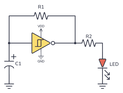
Before you start drawing wires and stuff, you need to know what circuit you want to build. So you need a circuit diagram.
You can either find one that someone else has made, or you can design your own from scratch.
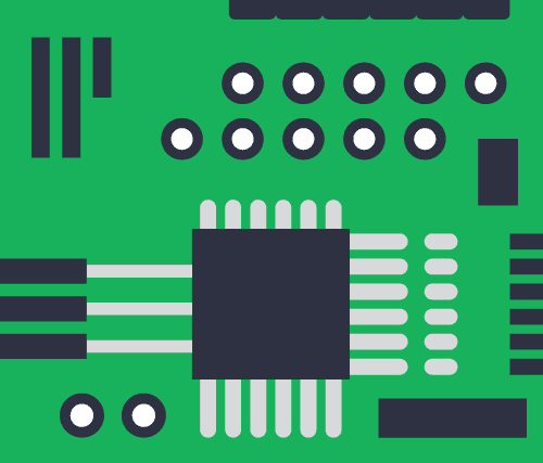
I recommend starting with something simple. Like this blinking LED circuit:

Once you have your circuit diagram, move on to step 2.
Step 2: Draw Your Schematics
First, you need to install a PCB design software.
I highly recommend KiCad for making your PCB. It’s free and it’s really good. I’ve also created a step-by-step KiCad tutorial for beginners. But the following steps are more or less the same, no matter what software you use.
Create a new project. Then draw the schematics from the circuit diagram you found in Step 1.

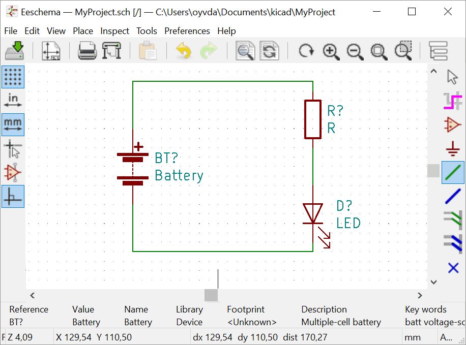
When you think you’re finished, run the Electrical Rules Checker (ERC) to see if you’ve made any errors.
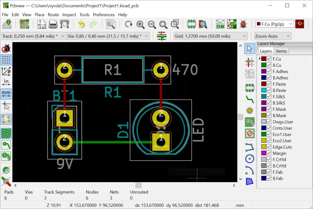
Step 3: PCB Design – Your Board Layout
Now it’s time to draw the board. You need to transfer your schematic diagram into a drawing of your printed circuit board.
This isn’t as hard as it might sound. Because the software will compare what you are drawing to the schematics file. And it will help you create the same connections.

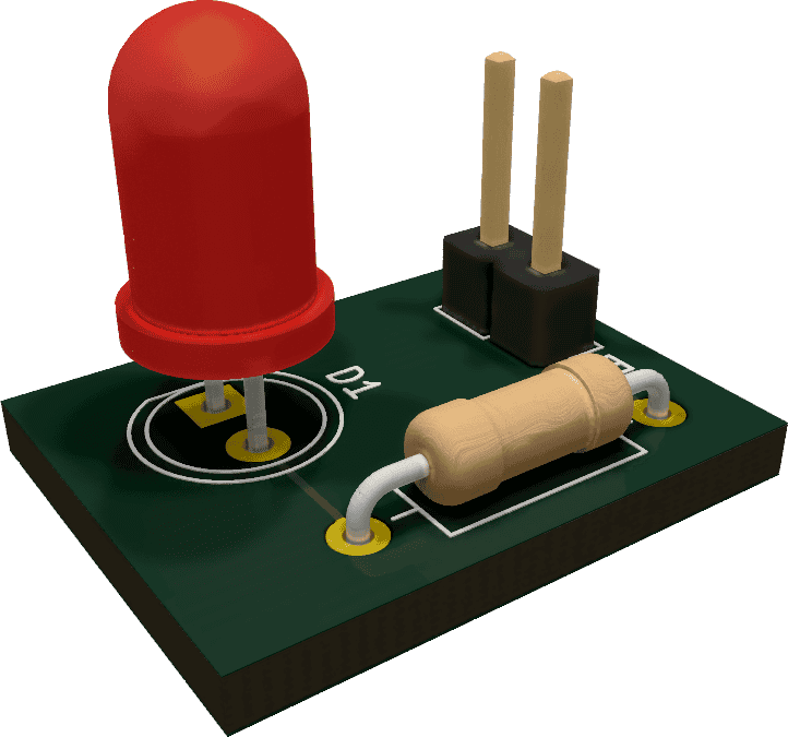
An important decision here is what footprint you should choose for the components. Through-hole or surface mount?
Through-hole components are the easiest to solder. I recommend through-hole for beginners. Surface mount components are smaller, so they take up much less space. But smaller also means it could be harder to solder. That said, it just takes a bit of practice to get used to surface mount components. So if you’re up for the challenge, then go for it.
Take your time, and make sure it looks good ;) Follow the design guidelines for drawing circuit boards.
When you’re done, run the Design Rules Checker (DRC) to see if you’ve made any errors.

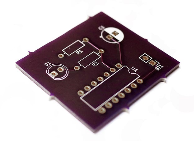
Step 4: Get Your PCB Made
When you’re finished drawing your PCB design, you need to get the design made. You could etch your PCB at home, but my preferred way is to just order a PCB from one of the many PCB manufacturers out there.
It’s really not expensive. For example, it’s not uncommon to see offers of 5 copies of your board for less than $5 USD! And you don’t have to mess around with chemicals on your own.
These are some of my favorites:
- OSH Park (Based in the US)
- Seeed Studio (Based in China)
- PCBWay (Based in China)
The classic way of sending a board layout to a manufacturer is by creating Gerber files from your design. But some (ex. OSH Parks) also accept KiCad files directly so that you don’t have to do any conversion.

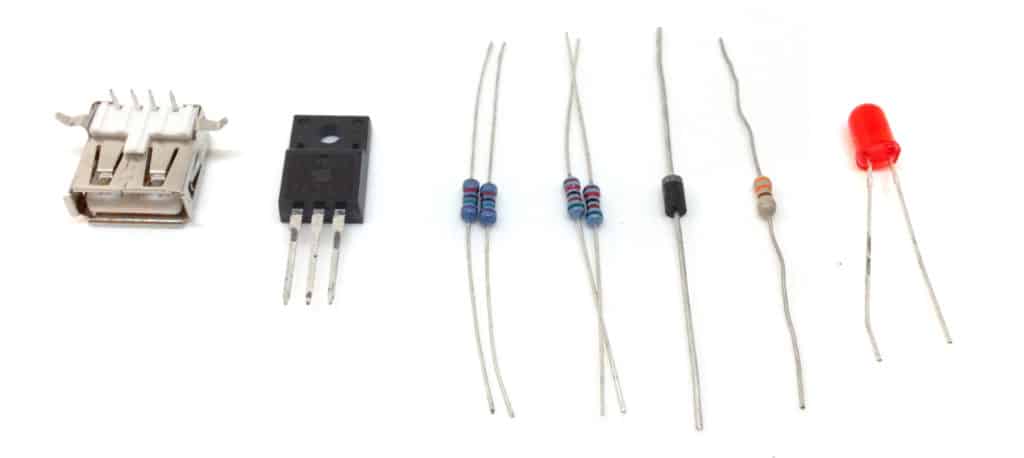
Step 5: Order Components
It usually takes a bit of time before your PCB is ready. So while you wait, make sure you have all the components you need. There’s nothing worse than receiving a fresh PCB, just to realize you are missing some key components!
I’ve put together a list of shops where you can buy electronic components online. The shops in that list I’ve either used myself, or I know someone who has used them.

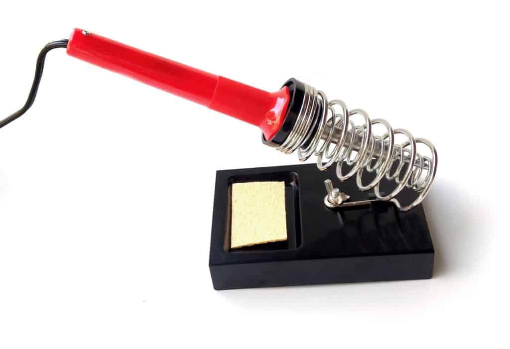
Step 6: PCB Assembly – Soldering the Components to the Board
You have your circuit board, fresh out of the printer. You have ordered and received the component. Now it’s time for the most exciting part – PCB upbringing!
Prepare your workbench and get your soldering tools out. Lay out the components and the PCB on your workbench.
Have your computer with the PCB Design close by so that you can check the orientation and value of components if needed. If that’s not possible, print out the schematic with values and the board layout.
Make yourself a cup of coffee, then get started soldering!

Questions?
What are your biggest concerns, doubts, or questions about PCB design? Is there something stopping you from making your first PCB? Let me know in the comment field below!
I need to replace (or repair) a Jandy Pool Heater circuit board. It has the identifying letters of PCB # 7417G. For Model LX400N-L Jandy Pool Heater … Serial # J06LG0853
Can you help me? Cost?
Thank You, Denis Vollom
Hi Denis Vollom,
Would you send the gerber file to [email protected], maybe we can help you.
Thanks.
Hi Jane,
can you give me the information about stencil drawing?
i can’t under stand what does stand for stencil in PCB?
Thanks,
Hi Samir,
Stencil is the copper pad which need solder.
Maybe you can email to me.
Thanks.
Hey Denis Vollom,
I think I might be able to help you, but you need to send email to us
[email protected]
Dear Denis Vollom,
How are you recently?
Do you have any PCB project recently?
We’d love to quote to you if you have,
My email is [email protected]
Wait for hearing from you.
Best Regards
Hebe
I can help
Can you please send related fiels and request to [email protected]? We can have a review and to see whether we can do that or not.
are u using common ground in your board……….plz check this website for any more
http://www.vestapps.wordpress.com
Also we can use Google Sketchup and Eagle up to render the design into 3D View.
HI
i want to design pcb.
actually i need power supply where in power is ac 100 to 300 v.
out put should be 24 v 2.5 amp DC.
can any one help
reply me on my email
[email protected]
hi Nikhil,
use bridge rectifier circuit.that only u wil conver 100v ac into 24 v dc
ok
Hi dear friend
I need your guidance, I need to have 160000 lux , pls kindly guide me about the necessary specifications for LEDs and lenses (number of leds, lense angle, …) and about cooling the LEDs (I’d like not to use heatsink).
I’m waiting for your reply a.s.a.p & I submit my best appreciation in advance
Best Reg.
reza
Make an earthing wire . it is probably because u are using the dc 12 v supply from a ac source
PLS send me a diagrame of DMX splitter amplifier for LED light controlling
thank you
sajeevan
Hi I am Jamil plz call me 03126763900
hi guys,
ı have a question . could someone help me?
ı need to learn how pcb circuit can build from curcuit.
ı mean think circuit there are electronics component and drawn on paper.
then drawn it from pcb.
may you contact with me from my e-mail address
e-mail: [email protected]
hi again
ı need construction given pcb circuit to normal circuit. these mayy any basic and easy circuit :)
thanks
e mail: [email protected]
hi am prince can someone help me on how to test a pc board where to begin together with the good name. of testing instrument. use my email for feedback at…………………………………….. [email protected]
Hi I am Jamil plz call me 03126763900
can anyone help me in designing my arduino development board along with some other accesories on a pcb design…
need help in pcb designing..
we can help you,please send email to [email protected],thanks.
sir m pcb pr ek compny m work krta hu pr mujhe ye smajh nhi aya ki folt kha h or m use kese pakdu plzzzzzz reply me
Pcb per kya work kerte ho
Describe for me the flow of current in a live wire on a circuit board
Please can anyone help.
I am trying to build a circuit board to control a standard wall fan. I need it to reverse polarity on motor( make it blow into room instead of sucking ) , also I need for it to run for only 2 mins every hour. This circuit board would run alongside the normal use of the fan, meaning priory would be given to its original intended use but if not used then my circuit board would work.
I am an electrician but don’t know hardly anything electronic, is there anyone who could help. Thank you
Gareth
I want to find the drill chart of the pcb , i having the gerber file of the pcb could u able to help get back me soon.
Would you sent me pcb designing software. [email protected] It’s my mail id. Plz sent that software
You can download it from http://www.cadsoftusa.com/download-eagle/
i want 24watts driver led bulb circuit diagram with out transformer it is very urgent
I WANT MORE INFORMATION TO DESIGNING A PCB
What help do you need in PCB.
Mail your query [email protected]
How we get the photo resistor lbr for using in eagle software.
Send me the link
hello sir my name is banoth sangya how to make mobile i want create one mobile how to do i am very interested that pour pas my no 8790171531
Sir, I motivated from you then decided to start my blog http://electronicsfxgeek.in/introduction-of-pcb-design-for-beginner/
Please suggest me to keep progress as a blogger.
That’s a helpful guide. Expecting more like this in future.
How to make schematic diagram for fire fighting robot using ardino mega 2560
Hai sir,
I am in need of reduction the size of pcb board.I am waiting for your reply sir.
Mail me your query
[email protected]
need help in pcb design
What help do you need in PCB Design
Hello
I’m actually making a solar power bank phone charging in which I need an MPPT charge controller. Can anyone of you please provide me with a schematic diagram for making this PCB board.
Thank you
email me on [email protected]
Keshav
Hi Keshav, I am Lily from China, We specialize in designing PCB assembly,Maybe I can help you! My phone number is +8613827439240 and email is [email protected]
Lily
Hi,
i need to learn pcb design,what are the steps need to follow. plz guide us
Hi,
i need to learn pcb design,what are the steps need to follow.
I Need basic for electronics,
which use for convert voltage and current
My Email Id:[email protected]
It might be worth considering EasyEDA.com for both a free EDA toolsuite and very low cost PCB fab and components supply?
As an EDA tool it is much easier to learn than Eagle and offers much more capability without needing to pay for the extra functionality.
continue more the is also interesting
interesting continue by this
Would you send the gerber file to [email protected]
Good evening sir. sir can i make ths pcb design in cadence tool
Yes.Very Thank you .And I Recommend a PCB online quote tool for you.
search:PCBindex
One of the best free PCB design packages available is KICAD. I have been using it for a few years now and it really works well. There are quite few tutorials available for kicad.
Thanks for this informative post!!!
According to me, to be a professional PCB designer, we have to be a part of IPC CID (Certified Interconnect Designer-basic) and CID+ (advanced) certification program. This professional development program provides an objective evaluation of core competencies in design, based on industry standards rather than specifications of just one company.
I want to design a digital printing device that prints on the walls or any base that we control on the computer
This information is very useful for me thank you so much I also want to design a circuit for my project can you explain me about Resistance please sir
Contact this company they will help you for any PCB Design: https://arshon.com/pcb-design
I am looking at designing a 2 layer PCB with through hole components that will sink 10 Amps of current. I understand that I need to make the width of my trace large enough to handle 10 Amps. My question is do i need to worry about the platting thickness on my platted through hole? The hole will contain the component lead and solder so does that negate the need to make sure the platting thickness will handle 10 Amps?
Very good tutorial comments and tips.
Anybody can help me how to route a 24ac – 60vdc dual converter schematic circuits on a wholed version board?
Thanks
This is so interesting! It’s difficult finding in-depth articles about PCB design. I’ve been doing research on OrCAD PCB Editors as well. Thank you for sharing!
Hello, I have a schematic for a PCB that I need built. I tried to design the board myself with various PCB design programs but have not been successful. Is there anyone or even a particular company you might recommend that can design the PCB for me and provide me with the Gerber files at reasonable cost? Thank you
You can post your project on upwork.com
If the schematic is 100% done and does not need any verification or changes, then it shouldn’t be too costly.
I down loaded the KiCad software, but it did not download the symbol library. Without that it is useless. Next to that, the link to the European PCB manufacturing showed prices of at leat 70 € for a small board if I buy 2. Not exactly cheap, so all in all a useless tool for me.
Yeah, you need the symbol library too. It should be a checkbox during installation. €70 is very expensive yes. You should be able to find $5-$10 alternatives. But the price of the board has nothing to do with the tool. You can purchase boards from anywhere with KiCad, it’s not locked into any manufacturer.
Hi.
Thanks for the wealth of information. I am looking for some to help complete the Motor controller design project that I started. Is there anyone who is interested in helping. I do not have much money to pay at this time, but sure can use the help.
Hello,
Can I start a business as freelance PCB designer.
Thanks,
WAF
Yes, absolutely. You can sign up for an account at Upwork and offer your services there.
Dear Øyvind Nydal Dahl,
I found your post on PCB design to be very informative and helpful. As someone who works in the electronics industry, I know how important it is to have a solid understanding of PCB design principles and best practices.
I especially appreciated your advice on the importance of starting with a schematic diagram and planning the layout of the PCB before getting started on the actual design. This is a critical step in the process, as it can help prevent errors and ensure that the final design meets all of the necessary specifications.
I also appreciated your discussion of the various software tools available for PCB design, and the pros and cons of each. It can be overwhelming to choose the right software for the job, so it’s helpful to have guidance on what to look for and how to evaluate different options.
One area where I have struggled in the past is creating high-quality PCB layouts that are both functional and aesthetically pleasing. Do you have any advice or resources for improving my PCB layout skills?
Overall, I found your post to be a valuable resource for anyone looking to improve their PCB design skills. Thank you for sharing your insights and expertise on this important topic.
Best regards,
Suriya