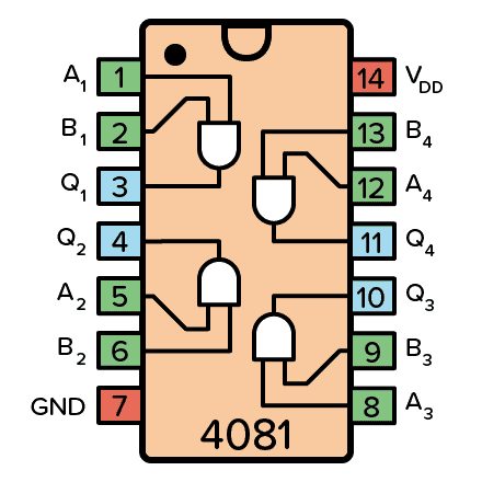
The CD4081 is a CMOS chip with four AND gates. An AND gate is a logic gate that gives a HIGH output only when all its inputs are HIGH.
This particular Integrated Circuit (IC) has four AND gates and each gate has two inputs. Therefore it’s often called a Quad 2-Input AND Gate.
Pin Overview
| Pin Name | Pin # | Type | Description |
|---|---|---|---|
| VDD | 14 | Power | Supply Voltage (+3 to +15V) |
| GND | 7 | Power | Ground (0V) |
| A1 to A4 | 1, 5, 8, 12 | Input | Inputs A of the four AND gates |
| B1 to B4 | 2, 6, 9, 13 | Input | Inputs B of the four AND gates |
| Q1 to Q4 | 3, 4, 10, 11 | Output | Outputs from the four AND gates |
What is an AND gate?
An AND gate is one of the basic logic gates. It can have two or more inputs. It gives a HIGH output only when all of these inputs are HIGH. The basic AND gate has two inputs and you can see its symbol and truth table below.

| Input A | Input B | Output Q |
| 0 | 0 | 0 |
| 1 | 0 | 0 |
| 0 | 1 | 0 |
| 1 | 1 | 1 |
How To Use the CD4081
To be able to use any of the AND gates in the chip, you must first connect the VDD pin and GND pin to the power supply. You’ll need a power supply voltage of anywhere from 3V to 15V.
Some versions of the chip support up to 20V. Check the datasheet of your version of the chip for exact values.
The A and B pins are the inputs to the four AND gates in the IC. What you input here decides the output.
The Q pins are the outputs from the AND gates.
CD4081 Example Circuit
Here’s a practical circuit example that you can build using a CD4081 chip.
Get the 555 Timer Cheatsheet
A super helpful reference that makes it easy to design circuits, so that you can build oscillators, timer circuits, and more in no time.
The circuit demonstrates the basic operation of an AND gate. A fun project for understanding the operation of an AND gate.
Normally, both inputs to the AND gate are pulled LOW by the resistor. Push any of the pushbuttons to create a HIGH on either input pin and see what the AND gate outputs. A lit LED represents a HIGH output. An unlit LED represents a LOW output.
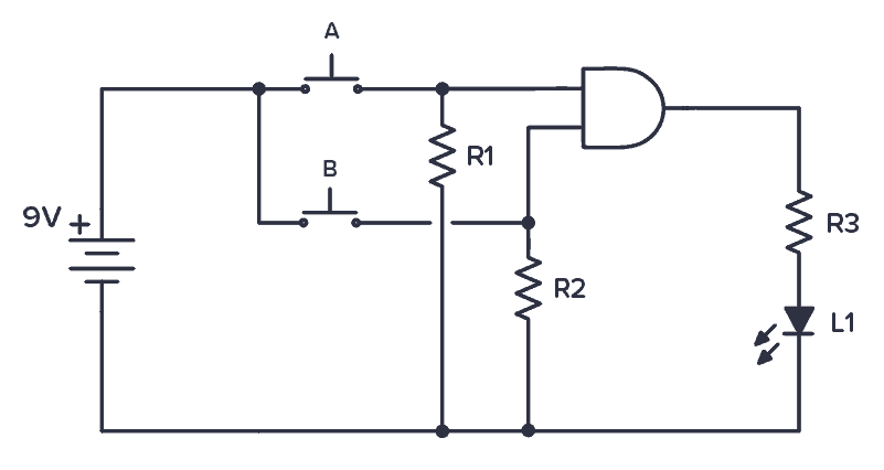
To build this you’ll need:
- Two pushbuttons
- A Red LED
- Three 10 kΩ resistors
- A chip with AND gates such as the CD4081BE
Connect the circuit as shown using any of the four gates available. For instance, pins 1 and 2 are the inputs to the AND gate with its output at pin 3.
But remember that you also need to connect the VDD and GND pins to your power supply in order for the AND gates to work – even though this is not shown in the circuit diagram.
Alternatives and Equivalents for 4081
You likely find the 4081 IC marked as CD4081, NTE4081, MC14081, HCF4081, TC4081, or HEF4081. Usually with a few extra characters at the end (Ex: CD4081BE).
This has to do with the manufacturer of the chip and the technology used. But the functionality and the pins are the same.
If you can’t find any of these in your local electronics store, check out my list of online stores where you can find components and tools for all your electronics projects.
Or try one of the following IC alternatives with 2-input AND gates:
- 74HC08: Quad 2-input AND gate
- 74HC09: Quad 2-input AND gate
4081 Datasheet
Download the PDF datasheet for the IC 4081 here:
CD4081B (Texas Instruments)
HEF4081B (Nexperia)
10 Simple Steps to Learn Electronics
Electronics is easy when you know what to focus on and what to ignore. Learn what "the basics" really is and how to learn it fast.