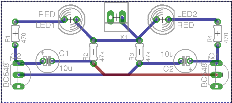
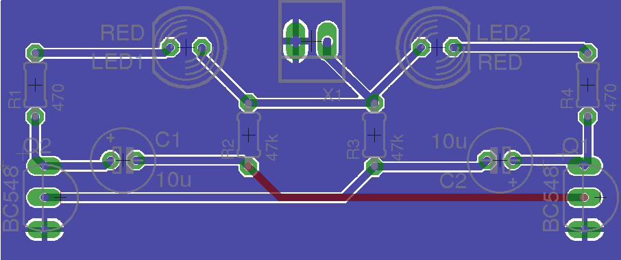
An Eagle ground plane is a plane of metal connected to ground. It is very useful for simplifying the routing of a board. If the major part of a layer is ground, you don’t need to design long traces to connect a pin to the ground.
[youtube http://www.youtube.com/watch?v=HO57DCDtgK0]
I was terrified of using planes in the beginning, because it seemed sooo complicated. But when I decided to try it out, I found that it was really simple :) Now I usually design boards with both ground plane and a positive supply plane. A positive supply plane can be constructed the exact same way as the ground plane, just make sure you give it the same name as the your positive supply (e.g. VDD).
An Eagle ground plane is constructed easily by using the “Polygon” tool. The following steps will explain how.
Step 1: Select Polygon Tool

Start with a board where you have routed all the signals except ground. Select the “Polygon” tool and use the parameter toolbar to set the layer, width and isolate values.
Layer

Choose the layer that you want your ground plane in.

Get Our Basic Electronic Components Guide
Learn how the basic electronic components work so that circuit diagrams will start making sense to you.
Width

The width has to do with the resolution of the Gerber files that will be created for manufacturing. If the width is too small, a lot of data will be created by the CAM tool. This is the recommendation from Eagle’s help menu:
“You should avoid using very small values for the width of a polygon, because this can cause extremely large amounts of data when processing a drawing with the CAM Processor.The polygon width should always be larger than the hardware resolution of the output device. For example when using a Gerber photoplotter with a typical resolution of 1 mil, the polygon width should not be smaller than, say, 6 mil. Typically you should keep the polygon width in the same range as your other wires.”
In this example, I chose 10 mils.
Isolate
The isolate value determines the distance between the polygon area and the other signals on the same layer. Make sure this is larger than the minimum trace space defined by your manufacturer. In this example, I chose 16 mils.
Step 2: Draw Polygon

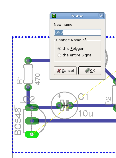
Draw a polygon over the entire board by left-clicking around the board.Use the “Name” tool to change the name of the polygon to “GND” (or whatever your ground signal is called).

Step 3: Calculate the Ground Plane
Now, when you click “Ratsnest”, the eagle ground plane will be calculated and visible.

If you close the board layout and open it again, the ground plane is no longer visible. If you want to see it again, just click “Ratsnest”.
If you don’t want to calculate and show the ground plane when using the “Ratsnest” command, you can turn it off with the command “SET POLYGON_RATSNEST OFF”.
For more information on the “Polygon” tool and how to customize your Eagle ground plane, type “HELP POLYGON” in the Eagle command line.
Return from Eagle Ground Plane Design to PCB Design

Get Our Basic Electronic Components Guide
Learn how the basic electronic components work so that circuit diagrams will start making sense to you.

