Before you send your board layout to PCB manufacturing, you should always check your board for errors.
There is a high chance of errors when you design a new board. And very often you don’t discover it before you have manufactured the circuit board and are trying to troubleshoot it.
If you’re able to remove all errors before you make the board, you’ll save a lot of time!
Many errors can be removed by making sure your schematic is correct.
When you’re sure your schematic is correct, there are a few other checks you should do to minimize the chances of any problems.
Tips Before Sending To PCB Manufacturing
Check for unrouted nets
When you are routing your board layout, one of the most common errors is to forget to route something.
You should always be 100 % sure that all your nets are routed before sending a board to PCB manufacturing. Unrouted nets on a finished board have caused me some serious headaches when troubleshooting my circuits.

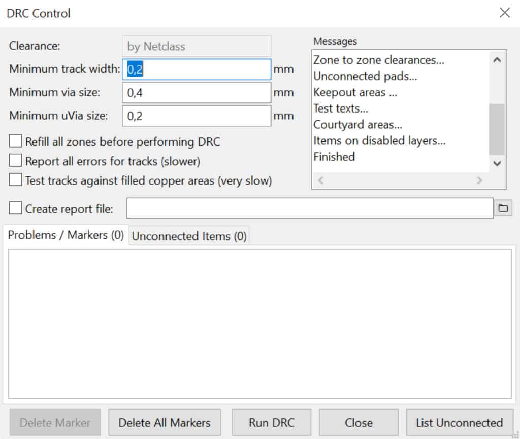
In KiCad you can check for unrouted nets by running the Design Rules Checker (DRC). You’ll find it in the Inspect-menu.

Make Your First Printed Circuit Board
Download my guide with all the steps you need to design your first printed circuit board (PCB) from scratch.
Click on the Run DRC button, then look for any unconnected nets in the Unconnected Items tab.

Schematic/board layout consistency check
Always make sure your board layout and schematic stay consistent, before you send it to PCB manufacturing. This means that their set of parts/elements and nets/signals must be equivalent. This consistency check is done by your PCB software.
In KiCad, you can make sure you have consistency by always using the Update PCB from Schematic... option under the Tools-menu. Or use this button on the toolbar:

Every time you make a change in your schematics, make sure you run this tool.
Check that you’re not breaking any design rules
The Design Rules Checker is also there to make sure your drill holes, trace widths, spacings and such are within the capabilities of your PCB manufacturer.
In KiCad, you can enter the values from your manufacturer in the Board Setup… window. You’ll find it in the File-menu.
Makes sure you run the DRC again after changing any values in the board setup.
Visually check your Gerber files
Create Gerber files from your board layout. In KiCad you can create Gerber files by choosing Plot… from the File-menu.
Then use a free online Gerber viewer to check your board visually for any mistakes. If everything looks ok, you are ready to send your board to production.
Choose a manufacturer that you like and follow their instructions on how to send them your Gerber files. This is usually done by email, a web uploader or through some custom software.
Some manufacturers, such as OSHPark and EuroCircuits, let you visually inspect your board when you upload your files. In this case, you can use their tools instead of an external Gerber viewer.
How To Learn PCB Design
If you haven’t already, I recommend strongly that you learn how to design your own circuit boards. It’s actually quite simple. Just check out my KiCad Tutorial on how to make your first PCB.
Return from PCB Manufacturing to PCB Design
More PCB Design Tutorials

Make Your First Printed Circuit Board
Download my guide with all the steps you need to design your first printed circuit board (PCB) from scratch.
