Here are some simple PCB design guidelines that can help you create better board layouts.
Board size and trace width
There are always limits to how big your board can be, how thin your traces can be and the smallest drill size you can use.
Start out by checking the capabilities of your PCB manufacturer. They usually put this information out on their web page. Sometimes they supply a Design Rule Check file that can be loaded right into your PCB design software.
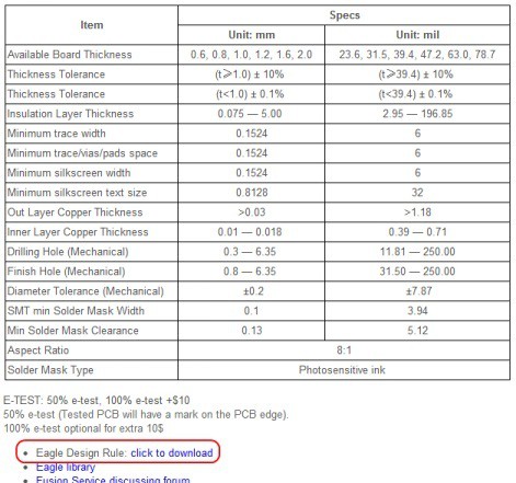
First, resize your board so that it does not exceed the capabilities of the manufacturer you have chosen.
Next, choose a trace width. It must be at least the size of the smallest allowed trace width, but should generally be thicker because thin traces are more vulnerable to damage when soldering.
The more current that is going to flow through the trace, the thicker it should be. This is to make sure the trace does not heat up. If you have a lot of space on your circuit board, start with 20 mil trace width for signals and 30-40 mil for power traces.
Placement of components
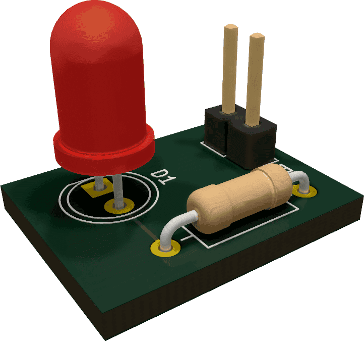
Place your components in a similar way as in your schematics. This makes it easier to troubleshoot your circuit if needed later on.
Pay attention to connectors and large components. Connectors should be placed on the side for simple connection.
Make Your First Printed Circuit Board
Download my guide with all the steps you need to design your first printed circuit board (PCB) from scratch.
If you are going to place the finished PCB in a box, keep in mind any large components and how they will fit in the box when you are going to assemble your electronic project.
If your electronic circuit consists of any decoupling capacitors, make sure you place them close to the pins they are meant for.
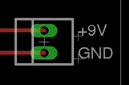
Use labels
Your components should all have labels with the name and part value printed on the board. This makes it easier to solder the circuit board and to troubleshoot it later on.
A useful rule-of-thumb is always to label connectors that are to be connected to the outside with descriptive names. Add names for each pin on a pin header.
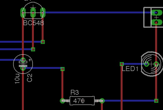
PCB design guidelines for horizontal and vertical routing
If you are using a two-layer circuit board, one of the best PCB design guidelines to follow is to route one layer horizontally and the other vertically.
For more complex boards, the addition of a ground plane can simplify your routing effort.
Trace angles
If you are making an RF circuit board, you should avoid 90-degree angles on your PCB traces. Otherwise, weird effects might occur.
Also, 45-degree angles look more professional, so you should just get into the habit of making 45-degree angles from the start.

Visual check
When you have completed your board, you should always print your board on paper and check it for any problems with connectors and such.
Many times I have done the mistake of putting a pin header the wrong way or something else that could have been avoided if I had just taken the time to print my circuit on paper and check for those things.
Return from PCB Design Guidelines to PCB Design
More PCB Design Tutorials
Make Your First Printed Circuit Board
Download my guide with all the steps you need to design your first printed circuit board (PCB) from scratch.
