In this Gerber tutorial, I will teach you how to create the files you need for a 2-layer board using Cadsoft Eagle. After you have completed this tutorial you will have all the necessary files needed to send to most PCB manufacturers.
This tutorial is out of date. I have switched to KiCad, so I recommend the updated tutorial How to Create Gerber Files in KiCad.
Step 1: Open the CAM Processor
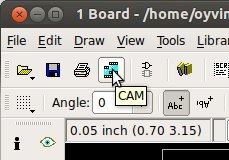
In Eagle, open Board view. Click the “CAM” button or choose “File->CAM Processor”. This will open the CAM Processor tool that is used to generate the files.
Here you can define the sections you want to create files for.
But you don’t really need to understand this. Actually I have never really thought about the details of this until I was writing this article. I have just been using ready-made configurations. And that is probably what you want to do as well.
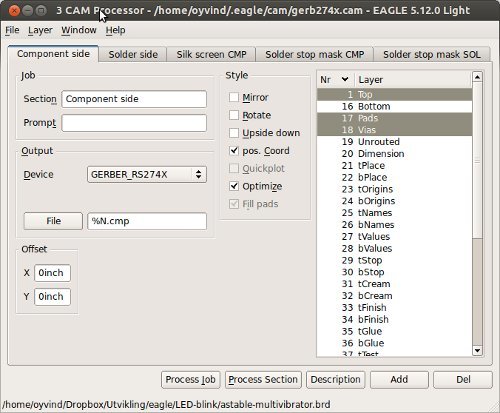
Step 2: Open a predefined job
To simplify creating Gerber files, Eagle comes with a predefined job for this. It is called gerb274x.cam.

10 Simple Steps to Learn Electronics
Electronics is easy when you know what to focus on and what to ignore. Learn what "the basics" really is and how to learn it fast.
(Note: If you want to order PCBs from Seeed Studio’s Fusion PCB service, you should instead download their own CAM-file from the bottom of their submission guidelines page. Be aware that this will give you different file names than the ones listed below in this article.)
To open it in the CAM Processor click “File->Open->Job…”
Browse to your …/eagle/cam/ folder, and you should see a file called gerb274x.cam. Choose it and click “Open”.
You will now see five tabs in the CAM Processor. Each of these tabs will generate a Gerber file.
Step 3: Adding a second silk screen (Optional)
If you look at the tabs, you will see that you don’t have a file for silk screen bottom. For simple boards, the silk screen is usually on the top layer so that you don’t need the bottom. Some of the cheap circuit board manufacturers don’t even allow bottom silk screen.
But if you need silk screen on bottom layer as well, follow these steps:
- Click “Add”
- Change Section to something like “Silk Screen SOL”
- Change File to “%N.pls”
- Deselect all layers
- Select layers 20 “Dimension”, 22 “bPlace” and 26 “bNames”
There you go.
Step 4: Create each gerber file
Select where you want to put the Gerber files by clicking on the “File” button and choosing a folder. Do this for all the tabs.
Then click “Process Job”. This creates your Gerber files.
Step 5: Adding file for drill holes
Even though drilling is supported by the Gerber format, manufacturers usually want the Excellon file format for specifying drill holes. Luckily, Eagle also comes with a predefined job for creating a drill file.
(Note: This step is automatically done if you’re using the CAM-file from Seeed Studio that I linked to in step 2.)
Open it in the CAM Processor by clicking “File->Open->Job…”
Browse to your …/eagle/cam/ folder, and open the file named “excellon.cam”.
Select where to put the output file by clicking on the “File” button.
Then click “Process Job” to create your Excellon file.
Step 6: Check output files
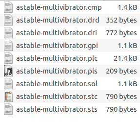
You should now have the following files:
- *.cmp (Copper, component side)
- *.drd (Drill file)
- *.dri (Drill Station Info File) – Usually not needed
- *.gpi (Photoplotter Info File) – Usually not needed
- *.plc (Silk screen, component side)
- *.pls (Silk screen, solder side)
- *.sol (Copper, solder side)
- *.stc (Solder stop mask, component side)
- *.sts (Solder stop mask, solder side)
After you have created each gerber file, you should always look at them using a Gerber viewer to make sure everything is ok.
Summary
This Gerber tutorial shows one way of creating the files you need. Even though this should be OK for many PCB manufacturers, you might find that some would want the files created in a slightly different way. If so, don’t worry, they will probably provide you with a Job file you can load directly into Eagle or at least have a good explanation on how to do it on their website.
Check out more articles on PCB design by clicking this link:
Return from Gerber File to PCB Design

Get Our Basic Electronic Components Guide
Learn how the basic electronic components work so that circuit diagrams will start making sense to you.
I would want to know more about circuit board, this is great, and am speechless about this.
I love this tutorial and it appears to be correct. Especially I appreciate the nuance about the separate process for generating the drill hole file.
It does not appear to work for boards that go to Seeed, though, since they expect different extensions. Any idea why that is, and whether they are just extension-renames of what this process produces?
If you don’t know, that’s fine; I’m just curious.
Hi,
You’re right, it seems like they have updated the extension names. Not sure if it’s just a matter of renaming it. But what you can do to get it correct it to download their Gerber generator file:
http://www.seeedstudio.com/document/rar/Seeed_Gerber_Generater_2-layer.zip
Unzip it, and use this file in Step 2 instead of the one I suggested.
Cheers!
Oyvind
This article is very useful, some of our customers said they followed the instructions and created the gerber files we needed for production. Really good. Best regards. Jeremy Q. from http://www.kejiepcb.com
Nice tutorial, this help me a lot!
Hi,
Very nice tutorial…
I would like to know one point…
which file describes Dimension of board details
Hi,
Thanks for the step by step tutorial, it is handy.
One thing I am wondering that wouldn’t there be a .gbr file as well?
Thanks.
You can set the file ending to whatever you want.
Best,
Oyvind
I’m actually following the instructions for Fusion PCB.
In the end I have all the files listed in step 6. But then what? I zip them and upload as is?
I think the author forgot this detail. For a beginner like me it’s not obvious what to do.
Thanks
Yes, just zip and upload.
Best,
Oyvind
Unfortunately I’m on x64 bit Win 10amd while Eagle 7.7 (free version) works fine, as soon as I initiate the CAM process it crashes the Eagle Program.
I’ve tried but no luck there. Bummer.
Any suggestions.
Have you tried installing the latest version (8.3.2 at the time of writing)?
Best,
Oyvind
but which device do you choose ?
mine is not listed which gerber format option should be considered standard
man these eacgle gerber cad tutorials suck ass
Eagle Gerba file generation has got to be the worst piece of software I have had the misfortune to use. Outdated confusing contradictory help files. If
Thank you for some good tutorials.
I’m using the most recent version 9.3.0 of Eagle where the CAM processor seems to have received a complete overhaul and looks very different to what is described here. Also, the mentioned gerb274x.cam file has been moved to a “legacy” folder. Is it recommendable to use this (legacy) file with new version of Eagle? If not, which of the new files should be used instead? Thanks.
Hi Thomas,
I am also having trouble generating gerbers, an luck for you?
Where do you want to manufacture your boards? If you are using Seeed Studio, check out this article: http://support.seeedstudio.com/knowledgebase/articles/1176949-how-to-generate-gerber-and-drill-files-from-eagle
If you are using someone else, check if they have a similar article.
Would you happen to have a more updated tutorial for the Eagle software (say, 2019?). Thanks mate! I attempted to follow your (2012) tutorial but after downloading the newest Eagle software, I noticed that it had been completely overhauled (understandably, since 2012, of course). Anyway, I got stock on step 5. Thanks again for taking the time to create such an informative and practical tutorial!
I’ve switched to KiCad, so I don’t unfortunately. Sorry!
Thank you very much for the nice explanation,
all things are very easy when you know them but if not a lot of questions signs arise.
For me it was the first time to create a gerber file by my self. Usually my PCB company did it for me, so i was very uncerten if created a useful file.
Many thanks
PS you do a super job with your website very nice both dumps up !!!!