It is always good to know a bit of PCB terminology. Here is a reference table with the most common words.
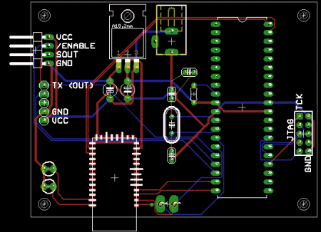
Bookmark it (Ctrl-D) and use it for when you stumble upon any PCB words that you don’t know.
| Term | Meaning |
|---|---|
| Thou | A “thou” is a thousandth of an inch and equivalent to a “mil”. |
| Mil | A “mil” is a thousandth of an inch and equivalent to a “thou”. |
| mm | “mm” is short for millimeter, a thousandth of a meter. |
| ESD | Electrostatic discharge caused by static electricity. |
| Trace | A path made of copper on a PCB. It is used in the same manner as electrical wires, to connect the components of a board. |
| Via | A hole with copper inside to provide electrical connection between a trace on one layer to a trace on a different layer of the PCB. |
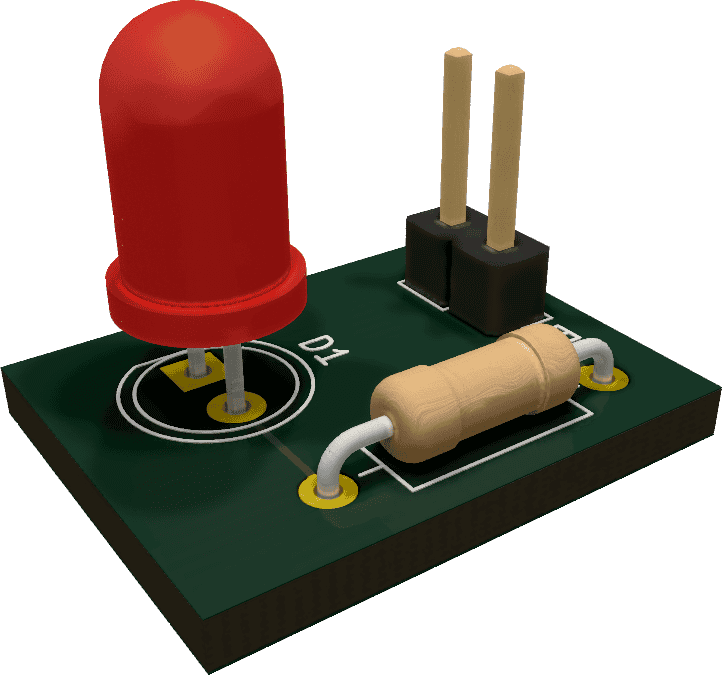
| Pad | Pads are used to solder surface mount devices to the board. |
| Annular Ring | The annular ring is the area that is left of a pad after a hole has been drilled in it. For example to make a solder pad for a through-hole component. |
| Silkscreen | Markings of component names, values and outlines on a PCB for simpler assembly and debugging. Usually white. |
| Solder Mask or Solder Resist | A substance that solder won’t stick to. Used to make sure traces are insulated electrically and physically. This is usually applied to the whole board except from where there are pads to be soldered. |
| Surface Finish | A layer on top of pads to prevent the copper layer from oxidation. |
| Gerber File | A file in the Gerber Format that is used as a universal way of telling manufacturers how to create your board. |
| Through-hole Components | Components that have leads which go through the board and are soldered on the other side. |
| Surface Mount Devices (SMD) | Components that are soldered on pads on the surface of your PCB instead of through holes. |
| Panelizing | Manufacturers often create one huge PCB with many identical board designs on it. The huge PCB is then cut into individual boards. This is called panelizing. |
| Single-sided PCB | A PCB with traces and pads only on one side of the board. |
| Double-sided PCB | A PCB with traces and pads on both sides of the board. |
| Multi-layer PCB | A PCB with traces and pads on both sides of the board in addition to traces on layers within the board itself. |
| PCBA | Some companies offer Printed Circuit Board Assembly (PCBA). This basically means that they solder the components to your board for you. Very convenient =) |
| FR-4 Substrate | The most commonly used material for creating PCBs. |
| RoHS | Restriction of Hazardous Substances. A European law intended to protect the environment. |
If you know the PCB terminology from the above table, you’ll understand most of my articles on how to build electronic circuits.
Learning To Build Your Own PCB’s
It’s super useful to know how to design your own circuit boards. It will help you build advanced projects like MP3 players, LCD Screens, Quadcopters, you-name-it.
I waited too long before I learned it. That’s why I created Ohmify, so that you can learn it now.
Click here to get access to the training.
Return from PCB Terminology to PCB Design
Make Your First Printed Circuit Board
Download my guide with all the steps you need to design your first printed circuit board (PCB) from scratch.
More PCB Design Tutorials
Make Your First Printed Circuit Board
Download my guide with all the steps you need to design your first printed circuit board (PCB) from scratch.
Sir I want to learn to making PCB please help me how to discuss with you and how to learn easily please tell me because this is my interested topic of life..and I want to learn any coast.
Hi, try this:
https://www.build-electronic-circuits.com/pcb-design/
Best,
Oyvind
I am trying to find out what the label “key” means on my TFT PCB.