The 74×114 (ex 74LS114) is a chip that includes two independent J-K flip-flops with clear and preset pins.
In this guide, you’ll learn the things you need to know about this chip in order to use J-K flip-flops in your own projects.
What does the 74HC114 / 74LS114 do?
The 74×114 is an integrated circuit with two J-K flip-flops. A J-K flip-flop is a type of digital storage element that can be used to store one bit of data. This IC allows you to set, reset, or toggle the output state based on the logic levels at its J and K inputs when a clock pulse is applied.

It also features a few additional inputs for each flip-flop:
- J and K Inputs: For controlling the operations (set, reset, toggle).
- Clock Inputs: Trigger changes based on the input signals.
- Clear Inputs: Used to reset the Q output to LOW.
- Preset Inputs: Used to set the Q output to HIGH.
These flip-flops are useful for building counters, shift registers, or for other applications that need to store and manipulate bits of data in digital electronics.
How To Use This Chip
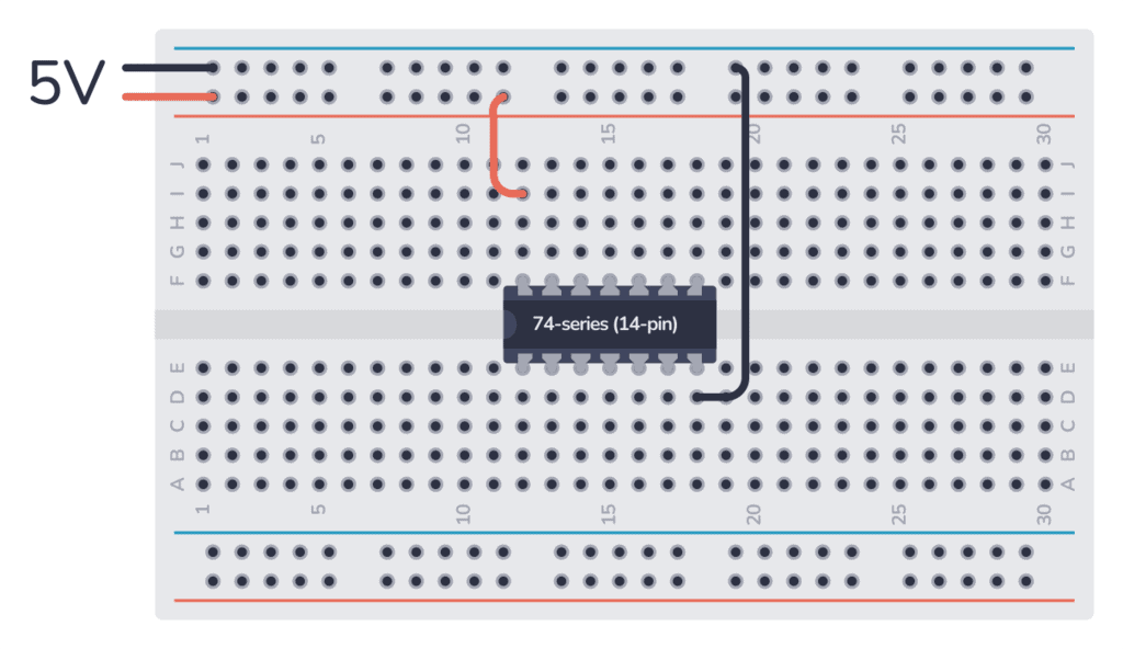
The 74×114 comes in a 14-pin package, and you need to connect it to power before you can use it. Most 7400 ICs support a VCC voltage of 5V. One difference between the HC and LS version of the chip is that the 74HC114 supports 2V to 6V, while the 74LS114 only supports 5V.
74HC chips can normally supply a maximum of 4 mA from an output pin. If you’re using the 74LS version, the maximum current you can pull out of one output pin is 0.4 mA when the pin is high (sourcing) or 8 mA when the pin is low (sinking).
But these values can differ between models, so check the datasheet of your model to verify.
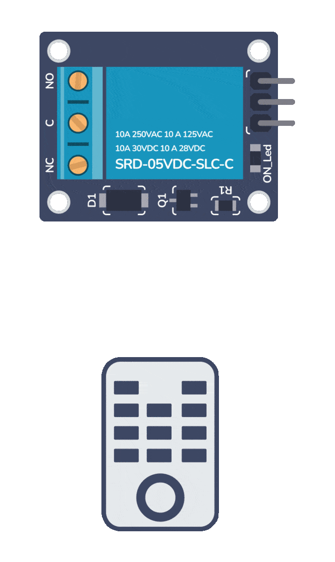
Build Something Useful This Evening
This gadget lets you use any IR remote-control to control your lamp, garden lights, heater oven, garage door, or anything else.
Once you’ve connected it to power, you can use the Dual J-K flip-flops inside.
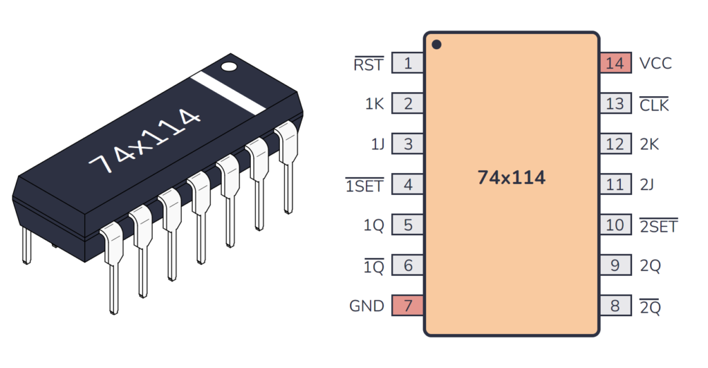
74×114 Pinout
The 74LS114 has 14 pins and contains two negative-edge-triggered J-K flip-flop with set, common clock and common reset laid out as shown in the pinout diagram below:
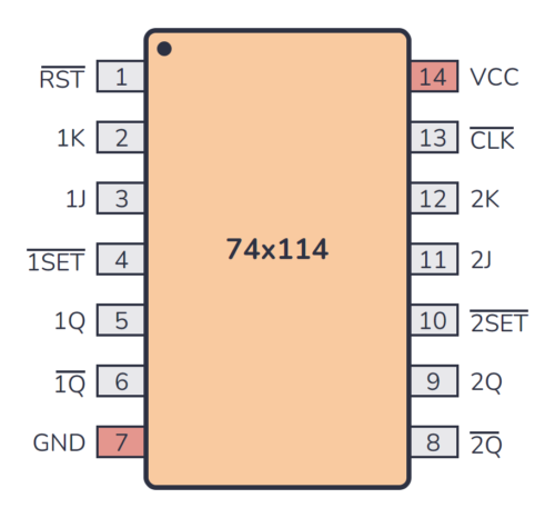
| Pin Name | Pin # | Type | Description |
|---|---|---|---|
| RST | 1 | Input | Reset input for both Dual J-K flip-flops (active low). |
| 1K | 2 | Input | K input for the first Dual J-K flip-flop. |
| 1J | 3 | Input | J input for the first Dual J-K flip-flop. |
| 1SET | 4 | Input | Set input for the first Dual J-K flip-flop (active low). |
| 1Q | 5 | Output | Output from the first Dual J-K flip-flop. |
| 1Q | 6 | Output | Inverted output from the first Dual J-K flip-flop. |
| GND | 7 | Power | Connect to ground (GND). |
| 2Q | 8 | Output | Inverted output from the second Dual J-K flip-flop. |
| 2Q | 9 | Output | Output from the second Dual J-K flip-flop. |
| 2SET | 10 | Input | Set input for the second Dual J-K flip-flop (active low). |
| 2J | 11 | Input | J input for the second Dual J-K flip-flop. |
| 2K | 12 | Input | K input for the second Dual J-K flip-flop. |
| CLK | 13 | Input | Clock input for both Dual J-K flip-flops (active low). |
| VCC | 14 | Power | Positive power supply. Connect to +5V power. |
Alternatives and Equivalents for 74HC114 / 74LS114
There are many versions of the 74×114 chip. They all have the same functionality, but with different specifications such as supported voltages and maximum current output.
Here’s a list of a few equivalents of this chip:
- 74HC114 (High-speed CMOS)
- 74HCT114 (High-speed CMOS, TTL compatible)
- 74LS114 (High-speed TTL)
- 74LVC114 (Low Voltage TTL)
- 74AC114 (Advanced CMOS)
- 74ALS114 (Advanced Low-Power Schottky TTL)
- 74F114 (Very High Speed)
- 74C114 (CMOS, similar to the 4000-series)
Some manufacturers also add a prefix, such as the SN74HC114 and SN74LS114 by Texas Instruments.
Can’t find the 74×114 anywhere? Then try one of the following IC alternatives:
- 74×67 – AND-gated master-slave J-K flip-flop.
- 74×70 – AND-gated positive-edge triggered J-K flip-flop.
- 74×72 – AND-gated master-slave J-K flip-flop.
- 74×73 – Dual positive-edge triggered J-K flip-flop.
- 74×76 – Dual J-K flip-flop.
- 74×78 – Dual negative-edge-triggered J-K flip-flop.
- 74×107 – Dual negative-edge triggered J-K flip-flop.
- 74×109 – Dual J-K flip-flop.
- 74×112 – Dual negative-edge-triggered J-K flip-flop.
- 74×113 – Dual negative-edge-triggered J-K flip-flop.
- CD4027 – Dual J-K master-slave flip-flop.
- CD4095 – Gated J-K flip-flop.
- CD4096 – Gated J-K flip-flop.
If you can’t find the 74×114 IC in your local electronics store, don’t worry, you’ll most likely find it in one of the stores listed on this page of online stores where you’ll find components and tools for all your electronics projects.
Datasheet for the 74LS114 and 74HC114 chips
Download the PDF datasheet for your version of the 74×114 here:
Get the 555 Timer Cheatsheet
A super helpful reference that makes it easy to design circuits, so that you can build oscillators, timer circuits, and more in no time.