This is a PCB design tutorial that I designed as a simple way to learn how to create a PCB layout in Cadsoft Eagle.
PCB Design is extremely useful to know. It’s what will take you from knowing how to build simple circuits to being able to build advanced stuff like LCD screens, Quadcopters, etc.
What you need for this tutorial:
- A computer with any version of Cadsoft Eagle installed
- A schematic diagram (Schematic Drawing Tutorial)
(If you want to use the same schematic as used in this PCB tutorial you can download the schematic here. You can also find three simple electronic circuits with schematics, board layout and Gerber files here.)
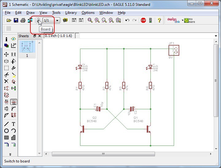
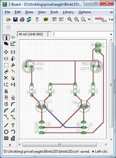
Create Board From Schematic
We start by opening our schematic diagram in Eagle. Click on the “Board” button (or choose “Switch to board” from the “File” menu) to create a board for this schematic.You can also use the command line for selecting commands.
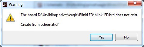
If no board exists, we will get a warning asking us to create a new board. Choose “Yes”. A new board will be created with all the components from the schematics.
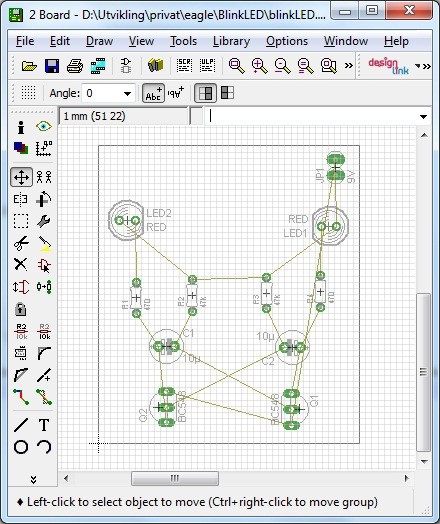
Place Components
We choose the “Move” action from the toolbar (or the “Edit” menu) to place the components on our board. A good way to arrange our components is to place them similar to the placement in the schematics. This makes it much easier to troubleshoot the circuit at a later stage if needed.
Click on “Rastnest” from the “Tools” menu to update the yellow airwires.
10 Simple Steps to Learn Electronics
Electronics is easy when you know what to focus on and what to ignore. Learn what "the basics" really is and how to learn it fast.
Start Routing
Alright, now the routing fun begins :)
Routing can be done manually or automatic. Here I will explain how to do it manually. You can also read about how to use Eagle’s autoroute function.
Choose “Route” from the toolbar (or from the “Edit” menu). Select 12 mil trace width and 24 mill drill size.
A rule-of-thumb is to use wide traces for nets that draw a lot of current, for example your power lines. For other nets, we can use thinner traces. In this example, not much current is drawn by the circuit, so we just choose some default values.

We start routing by clicking on one of the yellow airwires. A trace appears with a color corresponding to the current routing layer. Now we use our left mouse button to route the wire to where the airwire points us.
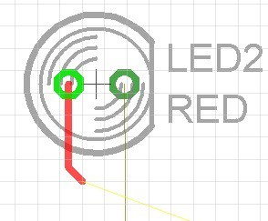
If we want to change the routing layer, we simply click the middle mouse button or use the layer selector on the toolbar. A good rule-of-thumb for a two-layer board is to route only horizontally on one layer and only vertically on the other. But this is not necessary for such a simple board as ours.
Learn more about PCB design guidelines.
To simplify routing, a ground plane can be added.
Run ERC and DRC To Check For Errors
When we are finished routing the PCB, we should always run ERC and DRC from the “Tools” menu to look for errors. Fix any errors if present.
When there are no more errors, we have finished the PCB design tutorial. Let’s give ourselves a pat on the back!
Now we are ready to create gerber files that we can send to a manufacturer for fabrication. Learn more about sending your design to a manufacturer here.
Return from PCB Design Tutorial to PCB Design
Get Our Basic Electronic Components Guide
Learn how the basic electronic components work so that circuit diagrams will start making sense to you.
Thank for rmail for me and I have some problem in create new libr. Io make Led 8mm (round) and
polygon ,ratness and Ripup two signal and ground plane. If reply pleased send to myu email address. Thank for kindness.
Sincerely yours,
BNambang Sutikno
[email protected]
Hi, it seems like you have a lot of questions. I think it’s better if you ask one at the time. I don’t really understand what you are asking.
Cheers!
Oyvind
what is the name and description for polarity and non-polarity capacitor in add tool in eagle software…?
Hi, may i know the function of this schematic diagram ? and what does it do after it becomes a PCB?
It’s an astable multivibrator, it’s two LEDs that will flash alternately.
Cheers!
Oyvind
hey oyvind!
I am working to build up a gps/gsm tracking device. i just have a schematic diagram of the circuit, can you please guide how it can be produced ?
Hey,
Check out this tutorial: https://www.build-electronic-circuits.com/schematic-drawing/
Cheers!
Oyvind
Hi!
I’m new to Eagle and your tutorial has been very handy! I just have one question: when you “start routing”, I can’t seem to be able to set the 12 and 24 values you are setting. The maximum value I’m allowed to set for WIDTH would be .254 and a DRILL of 0.12598425
Hey,
You’re probably using millimeter view. You can switch to “mil” by going to Edit->Grid…
Cheers!
Oyvind
I want to know the method for version 6.1.0
Hi! Is there any trick to design the layout of the board of an ECG circuit because I find it so complicated.
Hi Julie,
What exactly are you struggling with in the design?
Best,
Oyvind
Helpful site Oyvind! Thanks for putting this together.
Glad to hear that =)
Oyvind
hey,
Is there any Standards are available for selecting the PCB track thickness.(How much should be the track thickness for particular current)?
There are some trace width calculators out there that you can try. For example this one: http://www.4pcb.com/trace-width-calculator.html
Best,
Oyvind
Hi Oyvined,
My computer system is only 32 bit. Can it accept the Eagle Software?
Thanks,
Ding
I believe so…
How can I transfer my schematic and pcb design to a real pc board? I have to etch it myself.
Here’s the most common methods:
https://www.build-electronic-circuits.com/diy-pcb/
Best,
Oyvind
Hi sir, Can u help me do my pcb project?
If you have any questions, I’m happy to try and answer. But I don’t have the resources to do your project. If you need help with designing your project, try upwork.com